Packaging Innovation: China’s Bet on Advanced Chip Assembly

With lithography bottlenecks, focus shifts to breakthroughs in chip packaging and integration.
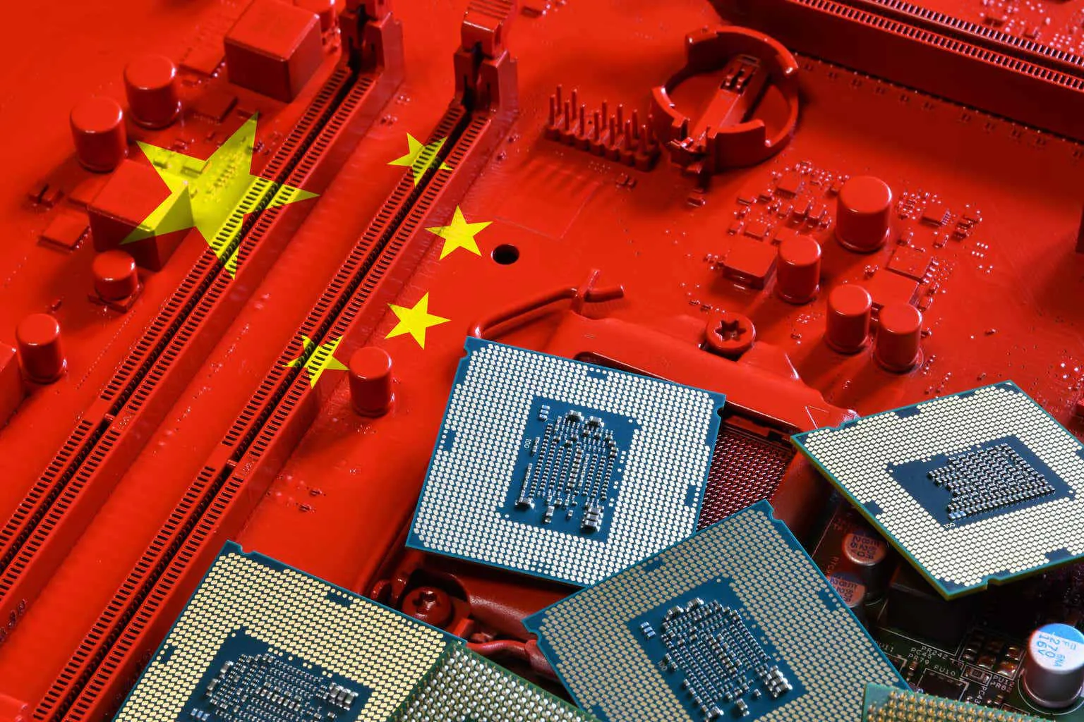
China’s semiconductor strategy in 2025 is increasingly turning toward advanced packaging, the process of stacking, interconnecting, and integrating chips to boost performance. With U.S. sanctions blocking access to the most advanced lithography machines, Chinese firms are exploring packaging as a way to narrow the gap with global leaders.
Companies such as JCET and Tongfu Microelectronics are spearheading research into 2.5D and 3D chip packaging, technologies that allow multiple chips to function as one high-performance unit. These methods can offset lagging progress at the nanometer scale by improving efficiency and reducing power consumption.
The government has recognized packaging as a strategic opportunity. Subsidies and industrial parks focused on assembly and testing are expanding in Jiangsu and Anhui provinces. Domestic demand is already strong, driven by AI accelerators, EVs, and smartphones requiring advanced integration.
While packaging cannot fully replace breakthroughs in lithography, it provides a pragmatic path for China to remain competitive. Success in this area could allow domestic firms to supply chips capable of supporting high-performance applications without cutting-edge nodes.